(I wrote this on Feburary 15th)
Today I fixed a bug in memory system and system that controls Central Unit's control signal. I made memory module for Von Neumann Architecture.
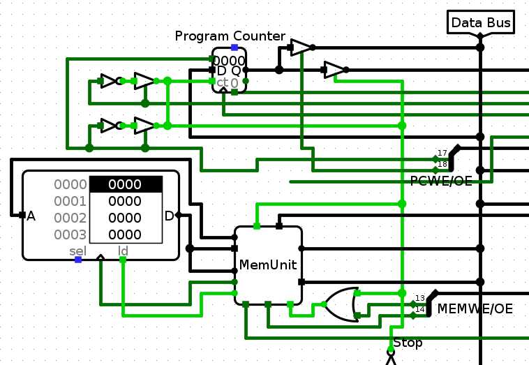
memory unit for the Von Neumann Architecture
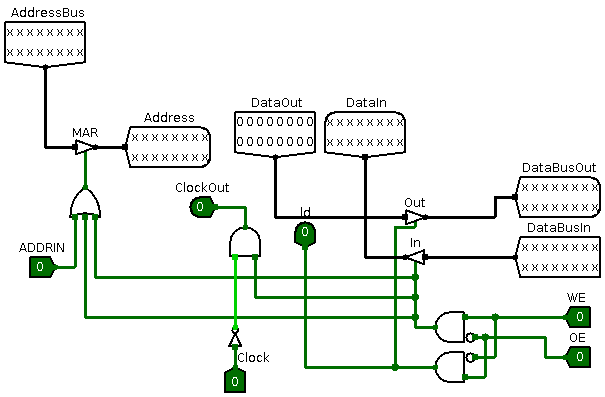
If we look at the MemUnit...
memory unit for the Von Neumann Architecture
...There's seven output and five input. The input consists of 'WE(Write Enable),' 'OE(Output Enable),' 'Clock' and 'ADDRIN.' What MemUnit does is that it controls when to emit the data to data bus. For instance, if we need to fetch the instruction from the memory, MemUnit automatically knows when to fetch the data, and emits data to the data bus. Also, if MemUnit receives some control signal that orders to fetch the data to bus, it automatically does that.
The data bus line is separated to Input and Output. Because RAM is a bidirectional component, I made two Input&Output wire for emitting data to Data Bus and writing data to RAM, respectively.
Here's some description for input&output pins.
Input pin (Excluding Bus inputs)
- WE(Write Enable) : A Control Signal that orders memory to write the Data Bus value to the address from Address Bus. When WE is high, data flows from Data Bus to RAM; that is, "In" buffer is opened. Because the RAM module requires clock signal to be written, ClockOut signal is activated by the WE signal.
- OE(Output Enable) : A Control Signal that orders memory to read the value from the Address Bus address. When OE is high, data flows from RAM to Data Bus, and "ld" signal is activated. The ld signal is signal that determines whether RAM should emit the value from the designated address(=A). For RAM to output the data, the 'ld ' pin should be high.
- ADDRIN(Address In) : Determines whether RAM gets the address from the Address Bus. In external side of system, this pin is connected to inverted "Stop" signal so that whenever the instruction is fetched, the address line is always open to Address Bus (.. cuz we need to fetch from the ram. Without address? we get nothing.) (Btw, the "Stop" signal is set to high when we fetched one instruction from RAM.)
- Clock : Raw clock signal from internal CPU clock.
Output pin
- ClockOut : (As mentioned before) ClockOut signal is activated when WE is high. When WE is high, the clock signal is directed to the ClockOut signal.
- ld(Load) : Selects whether the RAM should emit (on D) the value at the current address (A). (excerpted from Official Logisim Document)
Quite complicated.. even I cannot sometimes understand system that I Made..